Atomically Precise Manufacturing (APM) is an emerging manufacturing technology in which materials, structures, devices, and finished goods are fabricated such that every atom is positioned at an exactly specified location relative to the other atoms. In this method, the finished goods have no defects or imperfections.
Atomically Precise Hydrogen Resist Lithography (AP-HRL)
One method to achieve APM is tip-based atomically precise hydrogen resist lithography (AP-HRL). AP-HRL is the process of selectively removing hydrogen atoms from a passivated silicon surface using an atomically sharp point. An animation of AP-HRL is shown to the right in Figure 1. In this process, an electrical bias is applied to the probe and the resulting field ejects a hydrogen atom. By scanning the probe, a pattern can be created.
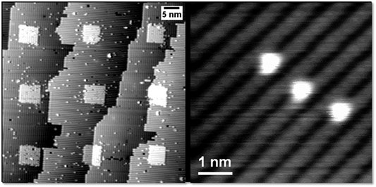
Tiptek is developing a high-yield process to manufacture probes for APM that are both sharp and have long performance lifetimes. Remarkably, Tiptek has demonstrated robust probe function in AP-HRL to create nearly 1,500 discrete features on a silicon surface without tip degradation. An example of this is shown in Figure 2.
Applications
APM is an entirely new kind of manufacturing; its potential technical, economical, and social benefits stem from its ability to enable the creation of materials and devices without defects at the ultimate limit of atomic scale precision. This new manufacturing capability is expected to lead to valuable new products for the electronics, energy, healthcare, and defense sectors in applications such as electronic devices, sensors, and quantum computing.
Figure 1: Animation of AP-HRL on a hydrogen passivated silicon surface.
Comments are closed.