Scanning tunneling microscopy (STM) and scanning tunneling spectroscopy (STS) are used to image and measure the electronic properties of surfaces, molecules, and nanomaterials.
Scanning Tunneling Microscopy (STM)
Based on quantum tunneling, STM images surfaces with atomic resolution using an electrically biased probe. This probe is brought in close proximity to a surface, and a bias voltage is applied, establishing a tunneling current. Holding the current constant, the tip is then rastered across the surface to obtain topography information.
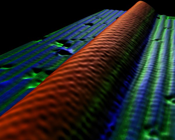
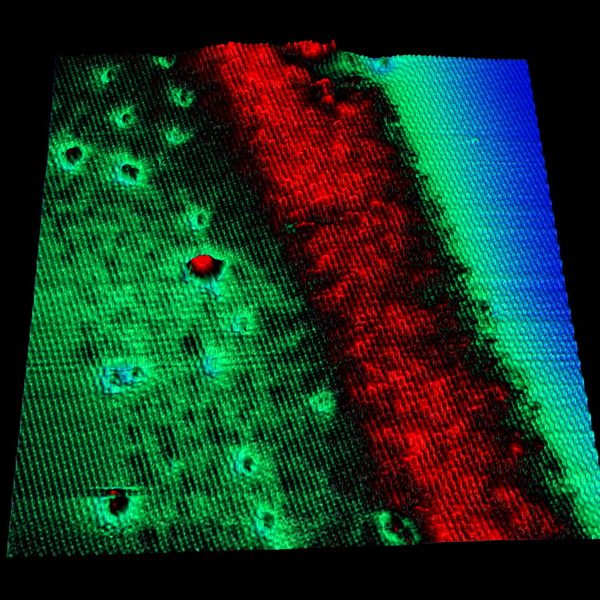
Figure 1 shows a UHV STM image of a single-walled carbon nanotube on a hydrogen-passivated silicon (100) surface. Figure 2 is a UHV STM image of a UHV-cleaved III-V compound semiconductor modulation doped (MODFET) structure. The different layers from left to right are GaAs, AlGaAs, InGaAs, and semi-insulating GaAs.
Scanning Tunneling Spectroscopy (STS)
STS is an extension of STM and used to obtain detailed electronic information which is essential when evaluating candidates for high performance electronic devices. In STS, the bias voltage applied between the tip and sample is varied. Information about local densities of states can be obtained from this method.


Comments are closed.