During the development and fabrication of semiconductors, engineers diagnose malfunctioning devices in a process called failure analysis (FA). This process deploys several analytical methods to verify that a failure occurred, determine the mode and root cause of the failure, and recommend a corrective action. Tiptek’s probes and needles are used in two of these methods: Nanoprobing and FIB/SEM lamella sample preparation.
Nanoprobing
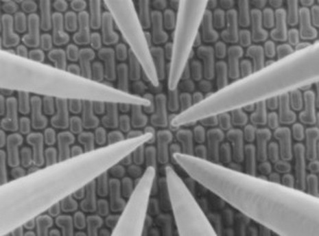
In today’s most complex integrated circuits, faults must be located among billions of transistors. To do so, the Failure Analysis engineer uses an instrument called a nanoprober to test electrical properties of individual regions on the chip. The nanoprober typically uses eight tiny probes to test current, voltage, and resistance of these regions. These probes are made up of a tungsten filament that comes to a sharp point that has a diameter of curvature of about 10 nanometers (nm) - small enough to touch and establish a conductive connection to critical contacts in the circuit. These probes allow testing of even the most advanced sub-3 nm node semiconductor technology.
The probes reside inside a scanning electron microscope (SEM) and are controlled by a precision piezoelectric nano-manipulator, which allows the engineer to place the probe in the desired location and provide an image of the surface. The probe plays a critical role in the nanoprobing technique – it must be hard, sharp, conductive, and able to survive multiple contacts with a surface.
FIB/SEM Lamella Transfer
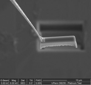
Once the fault has been isolated to a specific location using nanoprobing, the Failure Analysis engineer creates a thin micron-sized cross-section of the semiconductor chip, called a lamella, inside a Focused Ion Beam Scanning Electron Microscope (FIB-SEM). The engineer extracts this sample using the long and microscopically thin Tiptek LTN™ lamella transfer needle to deliver these cross-sections from the chip surface to a holder for subsequent analysis by transmission electron microscopy (TEM). In the FIB-SEM, a focused ion beam cuts out the cross section, a nanomanipulator moves it, and a scanning electron microscope allows the user to visualize the process.
Extra long and microscopically thin, Tiptek LTN™ lamella transfer needles provide many more transfer per needle than competitor products. In addition, they require no FIB milling for the first 30 transfers. These two features boost lamella throughput for the FIB-SEM operator by as much as 25% over traditional lamella transfer needles.
Comments are closed.