Tiptek STM Probes
Out of stock
Product Description
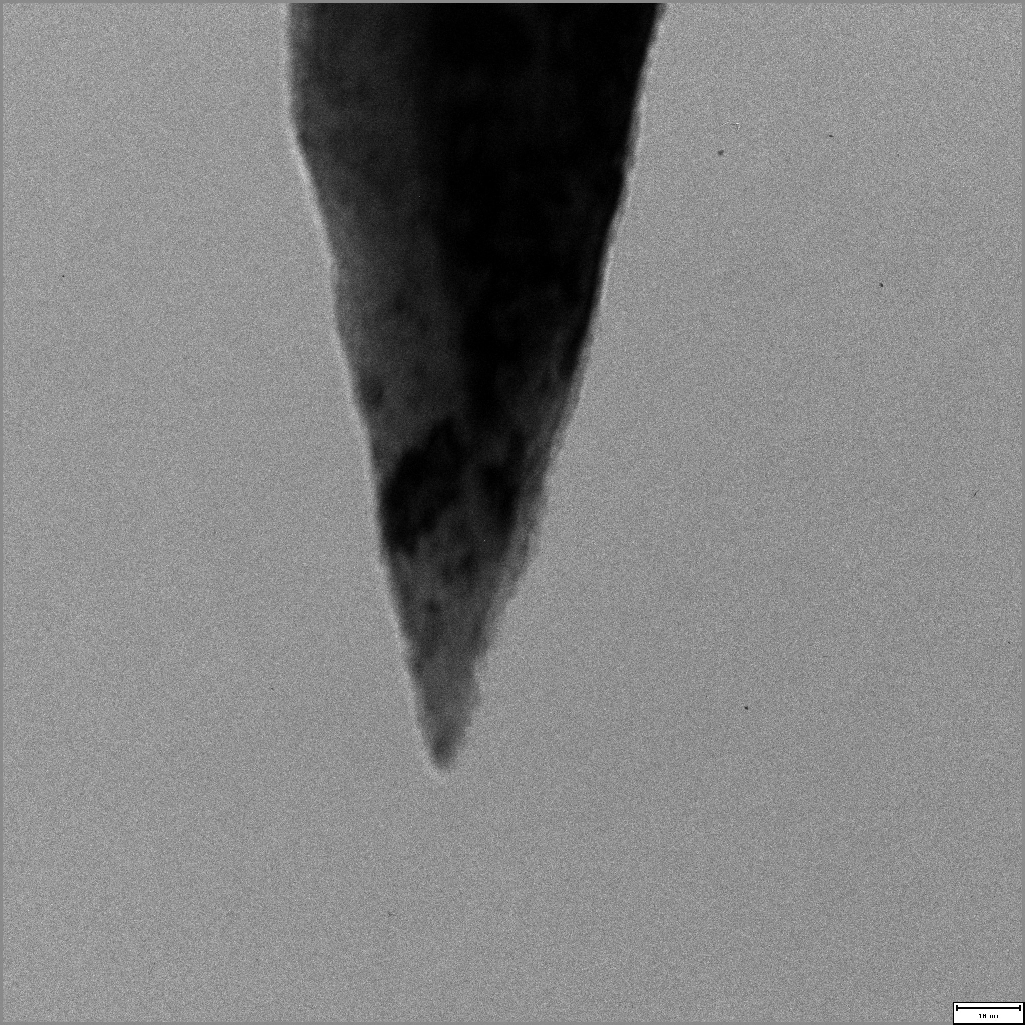
A Scanning Tunneling Microscope (STM) images a surface with atomic resolution using an electrically biased probe. In this technique, the STM user brings the probe in close proximity to a surface and establishes a tunneling current. While holding current constant, the probe is rastered across the surface and the relief map created from this motion is a direct representation of the atomic structure of the surface. At a given location, the user may also sweep voltage and obtain highly localized information on the electronic structure of the sample in a measurement call scanning tunneling spectroscopy.
Tiptek's ultra-sharp STM probes have the following characteristics:
| Material | Cylindrical Polycrystalline Tungsten |
| Probe Diameter | 0.25 mm |
| Length | 10-12 mm |
| Nominal Tip Radius of Curvature |
< 7 nm |
| Package Quantity | Box of 5 |