Product Description
NP Nanoprobes
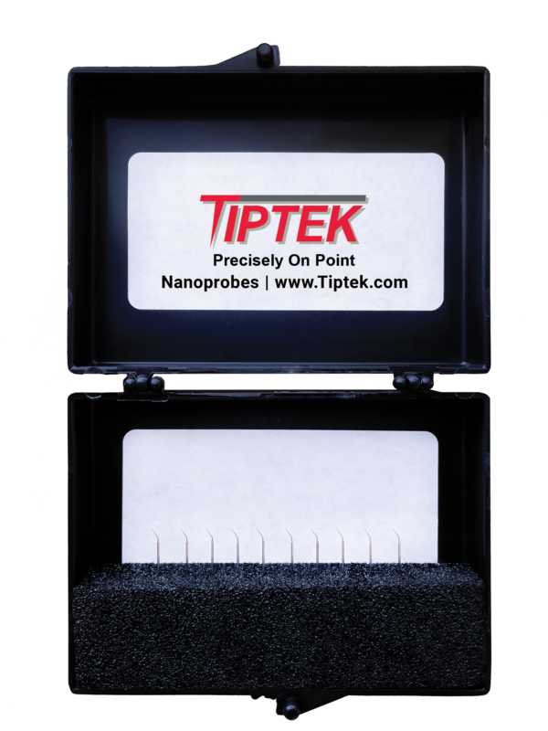
Tiptek’s NP nanoprobes are industry leading, tungsten-based probes with a hard, sharp, and conductive apex and a clean, debris-free probe surface. Tiptek offers a range of nanoprobe products for advanced and future technology nodes, electrical testing, and for nano and micro-manipulation.
| Features |
| Sharp |
Available with critical radii of curvature (ROC) as low as 1 nm for use in all advanced semiconductor nodes. Almond-shaped tip apices provides mechanical robustness and stability. |
| Long Life |
Hard tungsten-based probes provide numerous tip surface touches. |
| Low-Contact Resistance |
Materials of construction give metallic conductivity for accurate and repeatable electrical measurements. Probe resistance is typically less than 50 Ω after cross cleaning. |
| Long Shelf Life |
Packaged probes remain stable for a minimum of 6 months. |
| Robustly Packaged |
Vacuum packed in ESD-safe water/air barrier packaging to prevent ESD damage in transit and minimize oxide formation. |
| Widely Applicable |
Available for Thermo Fisher Scientific nProbers (II, III, and IV), Imina, Kleindiek Nanotechnik, and Hitachi nanoprober systems. Available in straight or bent configurations. Custom lengths and angles available. |
| Low eV Compatible |
Tiptek nanoprobes can be used for nanoprobing at voltages as low as 100 eV in Thermo Fisher Scientific nProber III and IV systems. |
| Benefits |
| Reliable & Consistent Results |
Tiptek nanoprobes are dependable and improve the output, accuracy, and speed of your failure analysis workflow. |
| Repeatable |
Tiptek probes are sharp and uniform for dependable results every time. |
| Timely Delivery |
Orders typically ship within 15 business days after receipt of purchase order. |
| Guaranteed Satisfaction |
If you are not fully satisfied with your use of Tiptek nanoprobes, we will replace them free of charge. |
Specifications
| Model Type |
NP-3 |
NP-5 |
NP-10 |
NP-20 |
NP-35 |
NP-50 |
NP-100 |
NP-250 |
NP-500 |
| Nominal ROC (nm) |
<3 |
<5 |
<10 |
<20 |
<35 |
<50 |
<100 |
<250 |
<500 |
| Wire diameter (mm) |
0.25 |
| Nominal Probe Length (mm) |
13 (depending on nanomanipulator system) |
*Custom bend angles and probe lengths available.
Contact for inquires: info@tiptek.com

